In the world of digital electronics, logic gates are the building blocks of all digital circuits. These gates perform logical operations on one or more binary inputs and produce a single binary output. One such gate is the NAND gate, which stands for “NOT AND”. In this article, we will explore the definition, symbol, truth table, and diagram of the NAND gate.
Definition of NAND Gate
A NAND gate is a logic gate that produces a LOW output (0) only when all of its inputs are HIGH (1). In other words, it is the opposite of an AND gate. The output of a NAND gate is the inverse of the AND gate’s output. This means that if the output of an AND gate is 1, the output of a NAND gate will be 0, and vice versa.
The NAND gate is also known as a universal gate because it can be used to implement any logical function. This means that any other logic gate, such as AND, OR, or NOT, can be created using only NAND gates.
Symbol of NAND Gate
The symbol of a NAND gate is a triangle with a small circle on the output side. The inputs are represented by lines entering the triangle, and the output is represented by a line exiting the triangle. The symbol is similar to that of an AND gate, but with a small circle added to the output line.
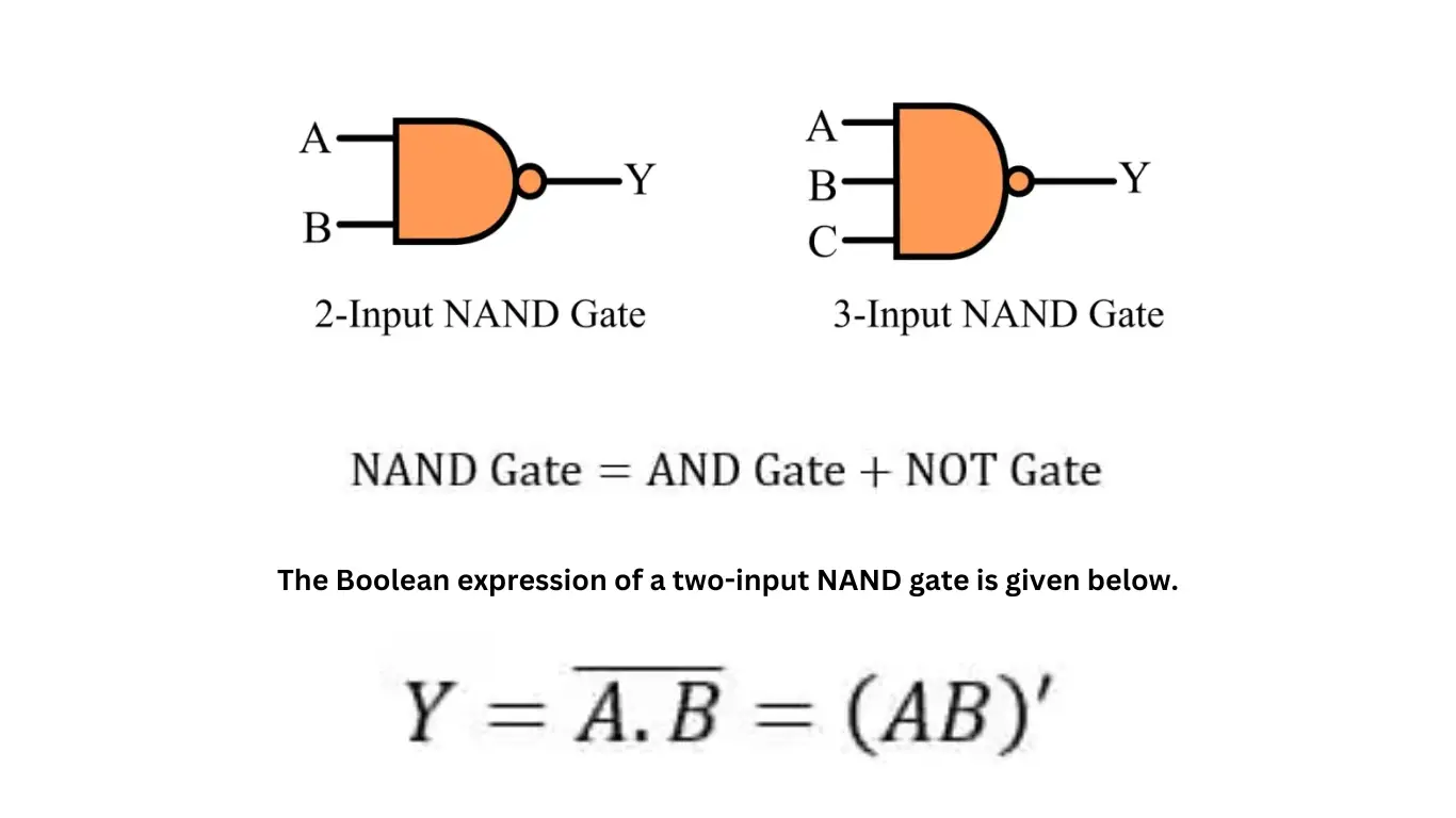
Truth Table of NAND Gate
A truth table is a table that shows the output of a logic gate for all possible combinations of inputs. The truth table for a NAND gate is as follows:
| Input A | Input B | Output | |———|———|——–| | 0 | 0 | 1 | | 0 | 1 | 1 | | 1 | 0 | 1 | | 1 | 1 | 0 |
As you can see, the output is only 0 when both inputs are 1. In all other cases, the output is 1.
Diagram of NAND Gate
A diagram of a NAND gate shows the physical implementation of the gate using transistors. A transistor is a semiconductor device that acts as a switch, allowing or blocking the flow of current. The diagram of a NAND gate is as follows:
The NAND gate is made up of two transistors, connected in series. The output is taken from the collector of the second transistor. When both inputs are HIGH, the transistors are turned on, and the output is pulled to the ground, resulting in a LOW output. In all other cases, the output is pulled to Vcc, resulting in a HIGH output.
Applications of NAND Gate
NAND gates have a wide range of applications in digital electronics. Some of the most common applications include:
1. Logic Circuits
NAND gates are used to create logic circuits, such as adders, subtractors, and multiplexers. These circuits are the building blocks of all digital systems, from simple calculators to complex computers.
2. Memory Devices
NAND gates are used to create memory devices, such as flip-flops and registers. These devices are used to store data in digital systems and are essential for the proper functioning of computers and other electronic devices.
3. Programmable Logic Controllers (PLCs)
PLCs are used in industrial automation to control and monitor machines and processes. NAND gates are used in the design of PLCs to create logic circuits that can perform various control functions.
4. Error Detection and Correction
NAND gates are used in error detection and correction circuits, which are essential in communication systems. These circuits detect and correct errors in transmitted data, ensuring the accuracy and reliability of the communication.
Conclusion
In conclusion, the NAND gate is a fundamental logic gate that is used in various applications in digital electronics. Its symbol, truth table, and diagram are essential to understand for anyone working with digital circuits. With its ability to implement any logical function and its use in memory devices and PLCs, the NAND gate is a crucial component in the world of digital electronics.
For more information, visit: Tech Me Life